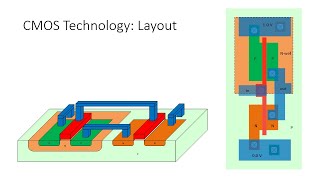
2 input nor gate stick diagrams for nmos ,cmos and bicmos inverters(1)
Published 3 years ago • 8.7K plays • Length 4:00Download video MP4
Download video MP3
Similar videos
-
 5:35
5:35
stick diagram for 2 input nand gate nmos inverter
-
 6:06
6:06
nmos inverter stick diagram
-
 9:04
9:04
stick diagram for 2 input nand gate for cmos inverter
-
 12:25
12:25
cmos nand gate | stick diagram | vlsi | lec-28
-
 12:50
12:50
cmos nor gate | stick diagram | vlsi | lec-29
-
 7:22
7:22
stick diagram of two input cmos nor gate || compact stick diagram
-
 7:12
7:12
cmos tech: nmos and pmos transistors in cmos inverter (3-d view)
-
 59:08
59:08
vlsi l29 stick diagram & euler's path 2021 07 13
-
 13:16
13:16
nmos design style
-
 14:46
14:46
cmos inverter | stick diagram | vlsi | lec-27
-
 9:19
9:19
m02 lec09 cmos 3 input nor gate stick diagram
-
 10:36
10:36
cmos nand gate stick diagram: circuit, design & working
-
 11:45
11:45
stick diagram of two input cmos nand gate || compact stick diagram || explore the way
-
 8:34
8:34
2 input nor gate design using nmos technology,how to design two input nor gate,2 input nor gate
-
 12:58
12:58
how to draw stick diagrams ?( vlsi )| simplified| with examples
-
 6:45
6:45
vlsid8-21 | bicmos logic | bicmos nand | bicmos nor | gate delays | vlsi design | vlsi | vlsi mannan
-
 6:48
6:48
m02 lec11 nmos design style inverter
-
 9:27
9:27
2 input nand gate design using nmos technology,how to design two input nand gate,2 input nand gate
-
 6:36
6:36
stick diagram of a boolean function || explore the way
-
 25:09
25:09
stick diagram ii cmos - mos circuit design styles - vlsi design
-
 12:43
12:43
cmos logic functions | stick diagram | vlsi | lec-30
-
 8:32
8:32
stick diagram for boolean expression using nmos transistor | vlsi design | s vijay murugan