how to place cavity regions in your pcb footprint
Published 1 year ago • 3.3K plays • Length 12:57Download video MP4
Download video MP3
Similar videos
-
 17:53
17:53
how to place embedded cavities in a pcb
-
 0:38
0:38
3 #pcbdesign strategies beginners should know #altium #electronics
-
 12:52
12:52
top 5 beginner pcb design mistakes (and how to fix them)
-
 10:40
10:40
6 horribly common pcb design mistakes
-
 12:26
12:26
top fifteen mistakes people make when designing prototype pcbs
-
 2:48:30
stm32 pcb design - complete walkthrough - altium designer & jlcpcb - phil's lab #41
-
 5:45
5:45
how to mate objects in your multi-board pcb's 3d assembly
-
 1:00
1:00
super pro esp32 rf pcb layout: one minute #pcbdesign review 05 #electronics #altium
-
 8:33
8:33
how to design rotation-proof connector pinouts
-
 59:27
59:27
navigating altium designer 20
-
 0:33
0:33
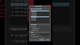
two ways to convert gerber files to a pcb layout #pcbdesign #altium #altiumdesigner
-
 38:01
38:01
altium pcb tutorial: from 0 to first board on osh park !
-
 6:29
6:29
pcb design process - the eda design approach - altium academy
-
 21:35
21:35
(2) introduction to multiboard pcb design - connectors - altium academy
-
 23:37
23:37
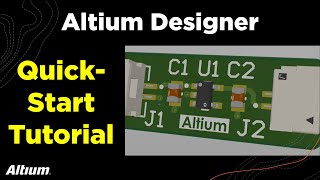
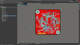
altium designer quick-start tutorial with phil salmony from phil's lab
-
 2:47
2:47
how to print your pcb in altium designer
-
 8:07
8:07
how to create footprint library | transformer footprint | part-2 | altium pcb design | tutorial 4
-
 6:15
6:15
how to create symbols and footprints in altium | pcb design tutorial