adeia semiconductor hybrid bonding technologies: wafer-to-wafer bonding
Published 1 year ago • 2.9K plays • Length 1:43Download video MP4
Download video MP3
Similar videos
-
 2:03
2:03
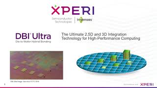
adeia semiconductor hybrid bonding technologies: dbi ultra
-
 3:04
3:04
adeia semiconductor hybrid bonding technologies: zibond and dbi
-
 3:16
3:16
discover: die-to-wafer hybrid bonding | cea-leti
-
 2:33
2:33
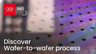
discover: wafer-to-wafer hybrid bonding | cea-leti
-
 23:01
23:01
inside micron taiwan’s semiconductor factory | taiwan’s mega factories ep1
-
 3:39
3:39
【半導體科普】台積電積極布局的 cowos 是什麼?ai 晶片大咖 nvidia、amd 都瘋搶
-
 15:18
15:18
삼성전자도 도전하기 시작한 '하이브리드 본딩'! 반도체 판의 물줄기가 바뀌고 있다.
-
 0:31
0:31
meet adeia
-
 3:12
3:12
discover: hybrid bonding | cea-leti
-
 1:11
1:11
the world of advanced packaging
-
 32:23
32:23
3d design and performance, dbi - enabled next generation soc architecture
-
 0:59
0:59
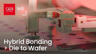
adeia semiconductor hybrid bonding technologies: die-to-wafer bonding
-
 0:25
0:25
webinar: hybrid bonding technology - today and tomorrow (short)
-
 14:40
14:40
packaging part 12 - hybrid bonding 1
-
 8:05
8:05
the power of the chip – up close and personal with hybrid bonding chip manufacturing
-
 4:30
4:30
ideas to innovations
-
 7:44
7:44
‘semiconductor manufacturing process’ explained | 'all about semiconductor' by samsung semiconductor
-
 0:48
0:48
no contact end-effector semiconductor wafer handling demo
-
 8:51
8:51
ev group explore die to wafer bonding and micro led technologies