cross probing in altium designer | pcb design tutorial | navigate windows to find specific component
Published 3 years ago • 704 plays • Length 7:33Download video MP4
Download video MP3
Similar videos
-
 0:49
0:49
auto cross-probing in altium designer 17 - pcb design software
-
 2:10
2:10
how to use cross select mode in altium designer
-
 6:28
6:28
altium - component placement (quick and elegant way) - cross probe
-
 5:39
5:39
altium - component placement & probing (the new & old way)
-
 21:12
21:12
to pour or not to pour | copper pour in pcb design
-
 15:34
15:34
i2c and spi on a pcb explained!
-
 17:00
17:00
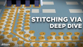
stitching via deep dive | pcb layout
-
 0:42
0:42
how to connect polygons to nets in altium designer
-
 2:38
2:38
how to utilize cross probe, masking, and highlighting in circuitstudio - altium academy
-
 2:50
2:50
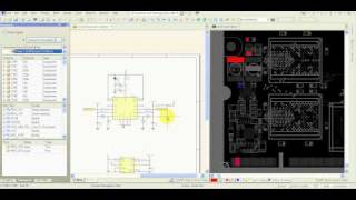
altium designer tutorial - nets / components browsing / probing in schematic and pcb
-
 3:45
3:45
how to create polygons in altium designer | pcb layout
-
 0:14
0:14
salsa night in iit bombay #shorts #salsa #dance #iit #iitbombay #motivation #trending #viral #jee
-
 0:30
0:30
how to flip component at altium schematic. #altium #mirror #component
-
 6:38
6:38
six basic design rules for any pcb design - altium whiteboard videos
-
 0:22
0:22
getting started with blind & buried vias #pcbdesign #electronics #altium