defect review semvision g7
Published 5 years ago • 2.8K plays • Length 2:24Download video MP4
Download video MP3
Similar videos
-
 19:35
19:35
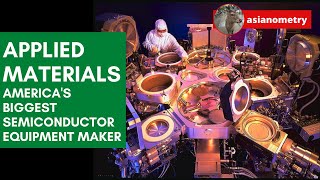
how applied materials became america's biggest semiconductor equipment maker
-
 6:28
6:28
ebeam 102: applications
-
 5:34
5:34
uvision 7 introduction
-
 5:16
5:16
‘semiconductor ecosystem’ explained | 'all about semiconductor' by samsung semiconductor
-
 17:13
17:13
intel in israel: a semiconductor success
-
 12:18
12:18
the big semiconductor water problem
-
 1:45
1:45
introducing a new playbook for process control
-
 12:41
12:41
semvision atp adc tier 2 300mm test
-
 1:00
1:00
surface master - the new standard of automatic metal surface inspection
-
 4:24
4:24
the semiconductor terms that you must know | 'all about semiconductor' by samsung semiconductor
-
 0:30
0:30
modular ai defect inspection solution makes semiconductor equipment upgrades more efficient
-
 2:13
2:13
plastic film tensile strength test astm d882
-
 4:26
4:26
things you didn’t know about semiconductor | 'semiconductor dictionary' by samsung semiconductor