stitching via deep dive | pcb layout
Published 1 year ago • 32K plays • Length 17:00Download video MP4
Download video MP3
Similar videos
-
 15:11
15:11
flyback converter design deep dive
-
 13:27
13:27
flyback converter design explained - what you need to know!
-
 0:38
0:38
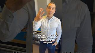
3 #pcbdesign strategies beginners should know #altium #electronics
-
 10:40
10:40
6 horribly common pcb design mistakes
-
 14:19
14:19
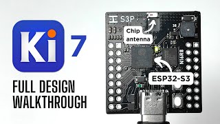
esp32-s3 chip antenna pcb - design your own in 15 minutes!
-
 7:58
7:58
esp32 in a commercial product? - from prototype to production
-
 6:27
6:27
flyback converter
-
 4:38
4:38
how to use via shielding and stitching tools in altium designer
-
 13:31
13:31
how to integrate skip vias in hdi pcb design
-
 0:59
0:59
tighter #routing on the passives! digital-to-analog converter 1-minute #pcbdesign #designreview
-
 3:32
3:32
creating, routing, and using new via types in altium designer
-
 7:18
7:18
via stitching and shielding | altium designer 17 advanced | module 11
-
 19:00
19:00
how to use blind and buried vias
-
 1:00
1:00
super pro esp32 rf pcb layout: one minute #pcbdesign review 05 #electronics #altium
-
 0:59
0:59
eliminate the pour! one minute #pcbdesign review 11 #electronics #altium
-
 3:26
3:26
pads to altium designer migration - defining micro vias
-
 1:00
1:00
power integrity issue? #designreview glitch-free 4-in-1 motor controller #electronicsdesign #altium
-
 21:39
21:39
how to reduce noise in pcb design
-
 14:12
14:12
return currents, effective via delay, round traces & more | q&a
-
 21:12
21:12
to pour or not to pour | copper pour in pcb design
-
 2:31
2:31
how to set up and use buried and blind vias | altium designer