eliminating nuances in the pcb manufacturing process
Published 2 years ago • 579 plays • Length 34:07Download video MP4
Download video MP3
Similar videos
-
 22:09
22:09
tolerances in pcb manufacturing
-
 32:58
32:58
the many benefits of additive process in pcb manufacturing
-
 9:14
9:14
pcb design release process - altium academy
-
 4:14
4:14
pcb origins during the ecad-mcad exchange | how to use altium designer
-
 10:06
10:06
return paths | mixed signal pcb design: part one
-
 10:40
10:40
6 horribly common pcb design mistakes
-
 30:43
30:43
how to cut and prepare blank pcb material before applying etch resist
-
 17:58
17:58
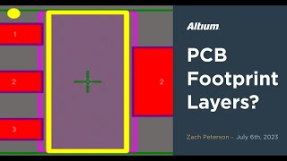
what's with all the layers in your pcb footprint?
-
 17:00
17:00
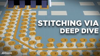
stitching via deep dive | pcb layout
-
 4:40
4:40
how to work with net classes in altium designer | pcb layout
-
 16:10
16:10
pcb dielectric materials construction | pcb manufacturing
-
 14:01
14:01
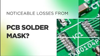
are there noticeable losses from pcb solder mask?
-
 0:12
0:12
iit bombay lecture hall | iit bombay motivation | #shorts #ytshorts #iit
-
 17:19
17:19
the easiest ways to reduce crosstalk in a pcb
-
 0:38
0:38
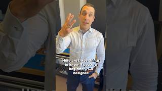
3 #pcbdesign strategies beginners should know #altium #electronics
-
 50:48
50:48
pcb component placement webinar
-
 12:52
12:52
top 5 beginner pcb design mistakes (and how to fix them)
-
 6:00
6:00
shaping the pcb | altium designer 17 advanced | module 9
-
 0:15
0:15
another pcb repair job in process with extra flux!
-
 6:29
6:29
pcb design process - the eda design approach - altium academy
-
 26:36
26:36
how to reverse engineer a pcb from gerber files
-
 0:47
0:47
introduction to rigid-flex pcb designs - altium academy