energy band diagram of pn junction explained by kushleen kaur
Published 4 years ago • 31K plays • Length 10:52Download video MP4
Download video MP3
Similar videos
-
 8:20
8:20
pn junction diode explained by kushleen kaur
-
 30:25
30:25
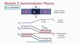
4.3 energy band diagram of pn junction
-
 14:25
14:25
energy band diagram of pn junction | electronics devices and circuits - edc
-
 11:24
11:24
reverse biasing of pn junction by kushleen kaur
-
 8:36
8:36
energy bands in solids (conduction band and valence band) by kushleen kaur
-
 13:54
13:54
semi conductors explained in brief by kushleen kaur, what are semi conductors, define semiconductors
-
 42:44
42:44
energy band diagram of pn junction diode by dr. rizwana
-
 11:49
11:49
p n junction (depletion region and energy bands)
-
 7:03
7:03
lec_23|energy band structure of open- circuited pn- junction diode
-
 5:03
5:03
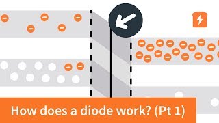
how does a diode work - the pn junction (with animation) | intermediate electronics
-
 11:31
11:31
law of the junction
-
 59:35
59:35
#24 | energy band diagram (pn junction) | edc | free crash course by shishir das sir | ec
-
 8:58
8:58
forward biasing of pn junction, forward biasing
-
 14:29
14:29
forward biasing and reverse biasing of p-n junction diode on the basis of energy band diagram
-
 7:50
7:50
pn junction band diagram
-
 33:27
33:27
energy band diagram in pn junction | energy barrier | potential barrier | bsc 3 | electronics | jam
-
 20:42
20:42
extrinsic semi-conductors explained in brief by kushleen kaur, what are extrinsic semi conductors?
-
 6:38
6:38
#energybanddiagrams #diode energy band diagrams of pn junction and depletion region | the primeguide
-
 59:13
59:13
mod-06 lec-06 energy band diagrams
-
 14:32
14:32
examples of energy band diagram of semiconductor | electronics devices and circuits - edc
-
 11:08
11:08
pn junction under forward bias condition (energy band, width of depletion region & characteristics)
-
 16:05
16:05
band theory part 2: energy band diagrams, lecture 7