ews100 - advanced optical inspection for semiconductor industry
Published 5 years ago • 1.5K plays • Length 2:03Download video MP4
Download video MP3
Similar videos
-
 1:18
1:18
ews300 microscopic wafer inspection
-
 3:14
3:14
how does automated optical inspection work?
-
 0:48
0:48
els 3600 - lens sorter & inspection system
-
 0:50
0:50
what is eddy current testing? || non-destructive testing course preview
-
 27:30
27:30
webinar: automotive aec-q100 early version
-
 17:26
17:26
eddy current testing
-
 5:14
5:14
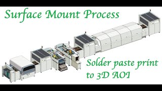
surface mount process - paste printing/inspection, component placement, reflow soldering & 3d aoi
-
 0:44
0:44
udm100 - de-panelling system smart solution for semicon packaging
-
 2:52
2:52
esl10™ e-beam wafer defect inspection system
-
 0:23
0:23
edingcnc atc function test @edingcncbv78 @sorotectv
-
 1:12
1:12
introducing optisure automated optical inspection (aoi)
-
 2:31
2:31
compliant array probe acfm solution
-
 2:30
2:30
advanced inspection solutions for semiconductor manufacturing.
-
 1:41
1:41
semiconductor manufacturing: wafer scribing using esi's ultrus system.