how does copper get inside of a via hole in your pcb - do you know this? (with kailey shara)
Published 3 years ago • 39K plays • Length 1:19:29Download video MP4
Download video MP3
Similar videos
-
 14:31
14:31
diy via plating - explained how copper gets inside of a via | kailey shara | #highlightsrf
-
 18:54
18:54
how gnd vias improve your pcb layout
-
 51:02
51:02
what every pcb designer should know - crosstalk explained (with eric bogatin)
-
 2:58
2:58
tip #090: crystals can be placed also on the opposite side of pcb, just keep the tracks short
-
 8:29
8:29
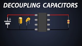
what are the decoupling capacitors? how to select decoupling / bypass capacitors?
-
 14:07
14:07
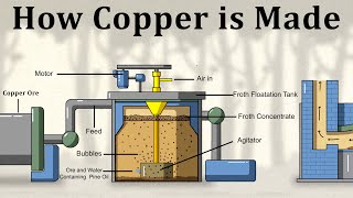
copper mining and manufacturing from the largest deposits in the world
-
 6:16
6:16
first attempt smelting copper ore the ancient way
-
 2:12
2:12
tip #011: don’t forget to place mounting holes on your board
-
 30:11
30:11
how to improve your pcb layout - vias
-
 1:39:34
how to design your pcb antennas and how antennas work (bluetooth antenna examples) - with john dunn
-
 5:03
5:03
how to build home office for 560€ in 3days
-
 30:31
30:31
what is the best via placement for decoupling capacitors?
-
 36:53
36:53
meet robert feranec - altium ontrack insight
-
 1:11:29
understanding crosstalk in pcb layout - you may wish you knew this before (with eric bogatin)
-
 52:32
52:32
how to improve your pcb layout - checking nets
-
 5:27
5:27
how copper is made animation | karthi explains
-
 1:32
1:32
how copper is produced
-
 54:06
54:06
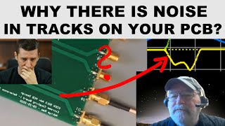
pcb layout & decoupling - measuring and fixing (part 3)