how to check pcb footprint vs real component
Published 4 years ago • 4.3K plays • Length 32:53Download video MP4
Download video MP3
Similar videos
-
 2:17:30
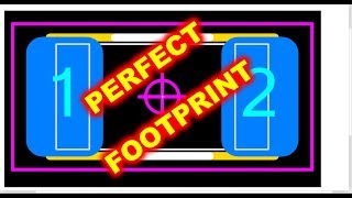
how to create perfect pcb footprint - what you really need to know
-
 36:37
36:37
i bought pcb footprint - was it worth it?
-
 6:41
6:41
tip #037: use “.checked pcb” ".checked sch" as component parameters
-
 17:58
17:58
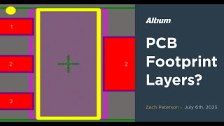
what's with all the layers in your pcb footprint?
-
 1:31
1:31
how to find any part (footprint symbol) in pcb editor or pcb
-
 10:40
10:40
6 horribly common pcb design mistakes
-
 49:24
49:24
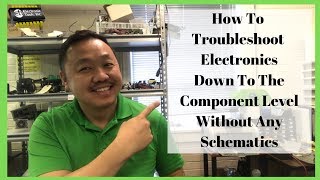
how to troubleshoot electronics down to the component level without schematics
-
 12:52
12:52
top 5 beginner pcb design mistakes (and how to fix them)
-
 5:08
5:08
how electronic boards are designed - explained in 5 minutes
-
 6:55
6:55
what is the right pad shape to use in pcb footprints? | tom hausherr | #highlightsrf
-
 3:58:52
🚨audio, gsm, gps, dac smartphone pcb design & components research🚨
-
 12:57
12:57
how to place cavity regions in your pcb footprint
-
 8:51
8:51
#6 how to select the right footprint for symbols in kicad 7.0 | #pcbcupid
-
 0:14
0:14
the right way to use a solder braid during pcb repair!
-
 1:00
1:00
how to get pcb footprint library of any electronics component #altium #pcbdesign #powerelectronics
-
 0:41
0:41
footprint - tools - check dimension
-
 15:11
15:11
review of a pcb layout: do you do same mistakes? - for beginners (part 1 of 4)
-
 0:38
0:38
3 #pcbdesign strategies beginners should know #altium #electronics
-
 5:26
5:26
altium tutorial - smaller clearance under bga or footprint
-
 2:06
2:06
how to import pcb symbols and footprint in your pcb - pcb design mastery course - lesson #11
-
 7:20
7:20
pcb footprint creation made easy (ipc compliant footprint wizard)
-
 5:12
5:12
tip #046: check pin ordering of your footprint