how to combine package and connector on pcb
Published 4 years ago • 3.2K plays • Length 4:09Download video MP4
Download video MP3
Similar videos
-
 6:47
6:47
how to combine pcb and package for hfss simulation
-
 11:16
11:16
how to connect two planar layout with bumps
-
 4:46
4:46
how to import pcb layout into hfss and make cutout
-
 6:17
6:17
how to wire up ethernet plugs the easy way! (cat5e / cat6 rj45 pass through connectors)
-
 29:24
29:24
how to remove electronic components - part 3 / soldering tutorial
-
 2:48
2:48
horizonrc.com how-to: ec3 connector installation
-
 7:18
7:18
design example: connector thru to package
-
 12:23
12:23
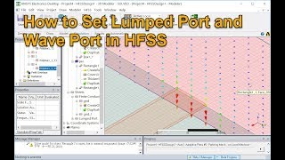
how to set lumped port and wave port in hfss
-
 15:16
15:16
how to: modeling of connectors, antennas and waveguides
-
 3:25
3:25
pcb connectors and electronics enclosures: connectivity technology for the future
-
 0:14
0:14
the right way to use a solder braid during pcb repair!
-
 9:52
9:52
how to estimate near field around package with circuit -electromagnetic co-simulation
-
 11:57
11:57
how to characterize and optimize connector-to-board transition designs
-
 0:46
0:46
pcb connection technology
-
 0:46
0:46
rf connectors - why so many?
-
 0:30
0:30
87549 connector 10mm 4 way 4 conductor solder less pcb
-
 1:10
1:10
quik strip multi connector for t & l connections in 8mm pcb led strip
-
 7:52
7:52
how to simulate emi of connector with push excitation