how to panelize your pcb design with ems expert kelly dack
Published 4 years ago • 2.7K plays • Length 46:03Download video MP4
Download video MP3
Similar videos
-
 2:47
2:47
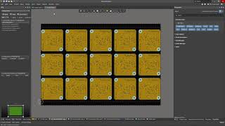
how to do panelization in altium designer
-
 12:49
12:49
to panelize or not to panelize
-
 11:26
11:26
sdg #138 how to panelize your pcbs
-
![what is pcb design? with kelly dack and judy warner [ontrack podcast]](https://i.ytimg.com/vi/UvkwdgmUYMs/mqdefault.jpg) 41:56
41:56
what is pcb design? with kelly dack and judy warner [ontrack podcast]
-
 10:40
10:40
6 horribly common pcb design mistakes
-
 1:08:17
walking through a big pcb factory in china | jlcpcb
-
 10:06
10:06
pcb panelization with kicad
-
 0:38
0:38
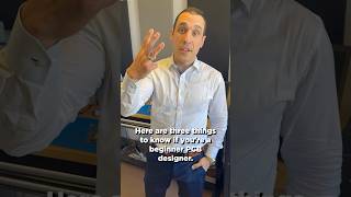
3 #pcbdesign strategies beginners should know #altium #electronics
-
 0:33
0:33
embedded board arrays at any angle | altium designer 21 what's new
-
 5:52
5:52
how to panelize pcb! | 40 pcb for just $2 | jlcpcb
-
 6:09
6:09
embedded board arrays and panelization | altium designer 17 advanced | module 21
-
 34:32
34:32
chris carlson's time saving tips for pcb design
-
 8:08
8:08
get 33% better efficiency on your pcb panels.
-
 6:29
6:29
pcb design process - the eda design approach - altium academy
-
 13:14
13:14
how to manually panelize pcbs
-
 4:15
4:15
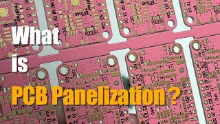
what is pcb panelization? | pcb knowledge
-
 55:18
55:18
panelization webinar june 2020
-
 55:18
55:18
panelization webinar - june 2020
-
 23:15
23:15
altium designer tips #8: pcb panel design in just 5 steps
-
 0:33
0:33
altium designer 21 - embedded board arrays at any angle