how to place cavity regions in your pcb footprint
Published 1 year ago • 3.3K plays • Length 12:57Download video MP4
Download video MP3
Similar videos
-
 17:53
17:53
how to place embedded cavities in a pcb
-
 17:58
17:58
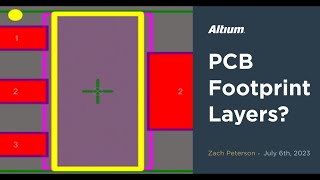
what's with all the layers in your pcb footprint?
-
 5:21
5:21
local pcb library & footprint creation in altium designer
-
 3:21
3:21
placing footprint pads in altium designer | component creation
-
 8:48
8:48
creating pcb footprints | altium designer 17 essentials | module 30
-
 12:52
12:52
top 5 beginner pcb design mistakes (and how to fix them)
-
 13:51
13:51
symbol and footprint creation | altium designer - phil's lab #31
-
 22:07
22:07
altium tutorial | 5.00mm capacitor footprint | altium footprint tutorial, pcb footprint, capacitor
-
 7:20
7:20
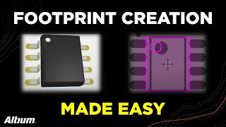
pcb footprint creation made easy (ipc compliant footprint wizard)
-
 17:09
17:09
how to create your own libraries in altium designer
-
 18:14
18:14
exploring paste mask & solder mask in your pcb footprint
-
 11:33
11:33
manual footprint creation with altium 365 | component creation
-
 2:54
2:54
creating a pcb footprint assembly drawing in altium designer | pcb layout
-
 17:57
17:57
altium 17: creating a component library (footprint and schematic)
-
 2:09
2:09
how to configure a pcb library in altium designer | component creation
-
 5:19
5:19
pads to altium designer migration - creating and using rooms
-
 2:27
2:27
creating a pcb footprint courtyard in altium designer | pcb layout