imaging of built-in electric field at a p-n junction by scanning transmission electron microscopy
Published 9 years ago • 571 plays • Length 0:43Download video MP4
Download video MP3
Similar videos
-
 4:36
4:36
imaging modes in transmission electron microscopy (tem)
-
 1:35:35
scanning electron microscopy - seeing is believing ? (all you need to know)
-
 57:50
57:50
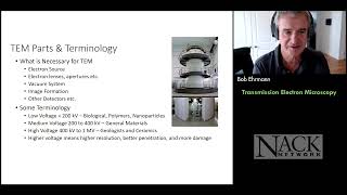
nack s14.2: transmission electron microscopy
-
 53:51
53:51
an electron microscope affordable for developing-world clinics?
-
 2:31
2:31
dynamic imaging with electron microscopy
-
 5:51
5:51
the world’s highest resolution electron microscope - hitachi
-
 4:32
4:32
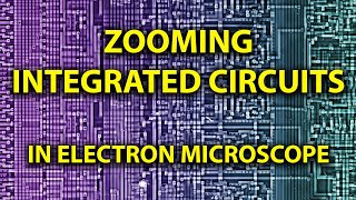
zooming integrated circuits with electron microscope!
-
 19:54
19:54
how do electron microscopes work? 🔬🛠🔬 taking pictures of atoms
-
 6:41
6:41
transmission electron microscopy
-
 3:19
3:19
scanning transmission electron microscopy explained
-
 2:53
2:53
transmission electron microscope
-
 21:42
21:42
scanning electron microscopy explained
-
 2:55
2:55
vise affiliated lab: brain imaging and electrophysiology network (bien) lab
-
 33:00
33:00
part 2 - workshop on 4d stem: fundamentals of electron diffraction & 4d stem, roberto dos reis
-
 36:50
36:50
electron microscopic imaging: past and future perspectives
-
 22:22
22:22
faculty241 phy445 kust20201 l9 p1 electron microscopy
-
 28:51
28:51
nanotalks - in situ tem as a powerful tool for studying a domain evolution in piezoceramics
-
 59:34
59:34
alan jasanoff: molecular probes for noninvasive neuroimaging
-
 1:21:13
electron microscopy - lecture 1, ncl 218 (ad) 2023
-
 9:44
9:44
pn junction electric field profile
-
 2:01
2:01
mechanical stimulation: integrated optical & atomic force microscopy l protocol preview
-
 37:00
37:00
bart koi (university of groningen)