impedance requirements: spi vs. usb
Published 2 months ago • 8.8K plays • Length 0:32Download video MP4
Download video MP3
Similar videos
-
 15:34
15:34
i2c and spi on a pcb explained!
-
 8:40
8:40
what is impedance? - altium academy
-
 12:17
12:17
altium designer rf impedance matching (e.g. 50ω, usb, ...)
-
 13:10
13:10
when to apply pcb termination
-
 4:00
4:00
why is 50 ohm impedance used in pcb layout? | explained | eric bogatin | #highlightsrf
-
 21:03
21:03
can you route usb 2.0 on a 2-layer board?
-
 4:22
4:22
easy altium guide to perfect impedance profiles (eg. usb, 50ω, ...)
-
 32:27
32:27
2-layer pcb design tips - phil's lab #137
-
 10:40
10:40
6 horribly common pcb design mistakes
-
 17:15
17:15
rf power amplifier design followup: pcb design
-
 6:20
6:20
controlled impedance routing - altium academy
-
 14:58
14:58
controlled impedance vs. controlled dielectric design
-
 17:08
17:08
why your impedance calculator is wrong
-
 21:51
21:51
how to design a usb to uart bridge with cp2102
-
 16:59
16:59
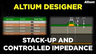
pcb stack-up and controlled impedance in altium designer
-
 14:11
14:11
impedance measurements using altium designer's signal integrity tool
-
 31:32
31:32
transmission line impedance calculation in altium designer - altium academy
-
 16:27
16:27
your quick guide to understanding pcb impedance tables
-
 14:10
14:10
fpga pins explained!
-
 3:22
3:22
how to apply impedance profiles using the rules and constraints editor
-
 14:28
14:28
what are differential pairs?
-
 0:38
0:38
3 #pcbdesign strategies beginners should know #altium #electronics