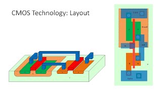
layout of 2-input cmos nand gate || p-well process || explore the way
Published 2 years ago • 15K plays • Length 6:33Download video MP4
Download video MP3
Similar videos
-
 7:28
7:28
cmos nand gate layout design | cmos vlsi mask layout
-
 9:07
9:07
layout of cmos inverter using p-well process || explore the way
-
 11:34
11:34
cmos 2-input nand and nor gates | layout diagram | vlsi | lec-34
-
 8:20
8:20
design of cmos logic gates ||simple and easy ||explore the way
-
 10:36
10:36
cmos nand gate stick diagram: circuit, design & working
-
 58:55
58:55
layout of two input nand gate in magic
-
 15:36
15:36
cmos logic circuit design for not, nand and nor gate
-
 18:56
18:56
cmos nand gate design | day on my plate | vlsi design tutorials
-
 11:45
11:45
stick diagram of two input cmos nand gate || compact stick diagram || explore the way
-
 11:24
11:24
design of cmos nand gate ||clear explanation ||explore the way
-
 12:23
12:23
cmos nand gate explained: circuit, working, implementation, and truth table
-
 18:03
18:03
cmos nand gate
-
 8:48
8:48
design of cmos nor gate || clear explanation || explore the way
-
 0:15
0:15
cmos nand gate layout #shorts #study #education #vlsi #layout
-
 6:36
6:36
stick diagram of a boolean function || explore the way
-
 7:45
7:45
cmos inverter layout design | cmos layout manochrome encoding
-
 11:40
11:40
2 input nand gate design using cmos technology,how to design two input nand gate,2 input nand gate
-
 15:41
15:41
2 input nand gate stick and mask layout design using cmos technology, how to design stick and mask
-
 7:12
7:12
cmos tech: nmos and pmos transistors in cmos inverter (3-d view)
-
 28:11
28:11
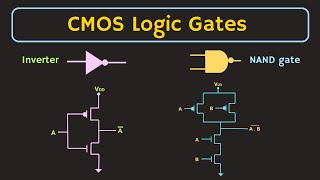
cmos logic gates explained | logic gate implementation using cmos logic