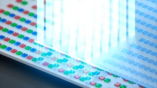
microled manufacturing process to debond from wafer and transfer to carrier using robots
Published 4 years ago • 11K plays • Length 1:19Download video MP4
Download video MP3
Similar videos
-
 2:25
2:25
coherent | microled laser processing for display production
-
 0:17
0:17
microled processing – laser-assisted bonding
-
 0:30
0:30
magazine to magazine leadframe transfer mechanism to laser marking chuck
-
 0:19
0:19
wafer ring blue tape laser marking
-
 7:21
7:21
microled wafertesting
-
 2:21
2:21
fully automatic glass wafer marking using laser
-
 0:43
0:43
flipping mechanism in laser marker machine
-
 5:01
5:01
coherent lasersystems | lasers are a key enabling manufacturing technology for microled displays
-
 0:22
0:22
bolite opto - high precision laser positioning and led repair
-
 2:40
2:40
high speed dual robot arm with dual laser marking station for marking bare semicon wafer.
-
 1:50
1:50
korean researchers to mass produce micro-led
-
 3:03
3:03
coherent | microled processing advanced laser solutions
-
 5:03
5:03
tno at holst centre | laser-assisted high-throughput microled assembly
-
 1:13
1:13
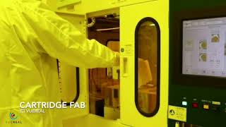
an introduction to vuereal's microled technology platform
-
 1:03
1:03
automatic operation compact wafer marker using robot arm for wafer transfer
-
 5:00
5:00
3d‑micromac | laser technologies for the production of microleds
-
 5:01
5:01
micledi microdisplays | microled display integration on 300mm advanced cmos platform