pcb layout fundamentals
Published 3 years ago • 24K plays • Length 42:38Download video MP4
Download video MP3
Similar videos
-
 42:38
42:38
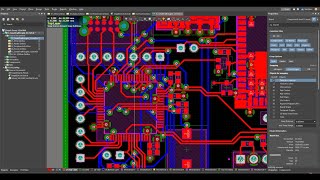
pcb layout fundamentals
-
 37:47
37:47
automated pcb parasitics extraction from eda tools for power electronics design support
-
 43:05
43:05
step-by-step snubber and clamp design for power supplies
-
 30:19
30:19
pcb traces 101 - phil's lab #112
-
 12:10
12:10
stability analysis of power supplies
-
 20:55
20:55
pcb production technology (full movie)
-
 10:40
10:40
6 horribly common pcb design mistakes
-
 8:08
8:08
printing pcbs at home!
-
 18:49
18:49
how to learn pcb design (my thoughts, journey, and resources) - phil's lab #87
-
 12:52
12:52
top 5 beginner pcb design mistakes (and how to fix them)
-
 50:59
50:59
webinar: input impedance and filter stability of dc/dc converters
-
 6:57
6:57
3 basic tricks for emc compliant pcb layout
-
 7:28
7:28
s-parameter & transfer function measurement
-
 16:30
16:30
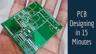
learn pcb designing in 15 minutes
-
 4:09
4:09
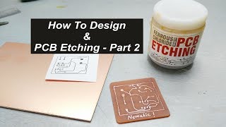
how to design & pcb etching- part 2
-
 3:55
3:55
how to design & pcb etching- part 1
-
 4:00
4:00
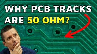
why is 50 ohm impedance used in pcb layout? | explained | eric bogatin | #highlightsrf
-
 54:06
54:06
pcb layout & decoupling - measuring and fixing (part 3)
-
 25:54
25:54
introduction to basic concepts in pcb design