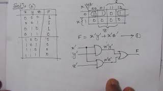
q. 4.1: consider the combinational circuit shown in fig. p4.1.(a)* derive the boolean expressions fo
Published 4 years ago • 49K plays • Length 13:35
Download video MP4
Download video MP3
Similar videos
-
 6:05
6:05
q. 4.2: obtain the simplified boolean expressions for output f and g in terms of the input variables
-
 8:17
8:17
q. 4.4: design a combinational circuit with three inputs and one output.(a) the output is 1 when
-
 6:28
6:28
q. 4.3: for the circuit shown in fig. 4.33 (section 4.11),(a) write the boolean functions
-
 29:44
29:44
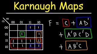
introduction to karnaugh maps - combinational logic circuits, functions, & truth tables
-
 18:14
18:14
q. 4.18: design a combinational circuit that generates 9’s and 10's complement of a bcd digit
-
 13:07
13:07
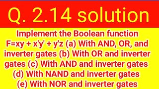
q. 2.14: implement the boolean function f=xy x'y' y'z (a) with and, or, and inverter gates
-
 11:23
11:23
q. 4.37: implement the following boolean function with a 4 * 1 multiplexer and external gates
-
 8:16
8:16
q. 4.6: a majority circuit is a combinational circuit whose output is equal to 1 if the input
-
 6:06
6:06
2.2.4 combinational devices
-
 6:12
6:12
q. 4.5: design a combinational circuit with three inputs, x, y, and z, and three outputs, a, b and c
-
 14:54
14:54
q. 3.22: convert the logic diagram of circuit shown in fig. 4.4 into a multiple-level nand circuit.
-
 15:38
15:38
q. 3.24: implement the following boolean function f, usingtwo-level forms of logic (a) nand- and
-
 10:28
10:28
q. 4.7: design a combinational circuit that converts a four-bit gray code (table 1.6) to a bit four-
-
 10:00
10:00
q. 6.7: draw the logic diagram of a four‐bit register with four d flip‐flops and four 4 × 1 multiple
-
 11:39
11:39
practice problems on combinational circuits (part 1)
-
 5:48
5:48
q. 4.35: implement a full adder with two 4 * 1 multiplexers.
Clip.africa.com - Privacy-policy