q. 6.11: a binary ripple counter uses flip‐flops that trigger on the positive‐edge of the clock.
Published 4 years ago • 20K plays • Length 15:09
Download video MP4
Download video MP3
Similar videos
-
 16:01
16:01
q. 6.12: draw the logic diagram of a four‐bit binary ripple countdown counter using(a) flip‐flops
-
 5:02
5:02
q. 6.15: a flip‐flops has a 10 ns delay from the time the clock edge occurs to the time the output
-
 4:22
4:22
q. 6.13: show that a bcd ripple counter can be constructed using a four‐bit binary ripple counter
-
 4:45
4:45
q. 6.14: how many flip‐flop will be complemented in a 10‐bit binary ripple counter to reach the next
-
 23:10
23:10
q. 6.17: design a four‐bit binary synchronous counter with d flip‐flops || complete design steps
-
 11:51
11:51
how to measure ripple voltage on a switch-mode supply - workbench wednesdays
-
 25:15
25:15
tsp #146 - teardown, analysis & repair of an agilent e3646a dual channel programmable power supply
-
 21:21
21:21
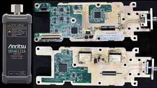
tsp #221 - anritsu ms46121a 6ghz usb vector network analyzer teardown & reverse engineering
-
 13:42
13:42
q. 6.28: design a counter with the following repeated binary sequence 0, 1, 2, 4, 6 use d flip-flops
-
 16:01
16:01
q. 6.18: what operation is performed in the up-down counter of fig. 6.13 when both the up and down
-
 23:32
23:32
q. 6.24: design a counter with t flip‐flops that goes through the following binary repeated sequence
-
 22:22
22:22
q. 6.9: two ways for implementing a serial adder (a b) is shown in section 6.2. it is necessary
-
 16:50
16:50
q. 6.27: design a counter with the following repeated binary sequence: 0, 1, 2, 3, 4, 5, 6. use jk
-
 15:02
15:02
q. 6.25: it is necessary to generate six repeated timing signals t0 through t5 similar to the ones
-
 17:11
17:11
q. 6.16: the bcd ripple counter shown in fig. 6.10 has four flip‐flops and 16 states, of which only
-
 10:00
10:00
q. 6.7: draw the logic diagram of a four‐bit register with four d flip‐flops and four 4 × 1 multiple
-
 10:22
10:22
q. 6.5: the four‐bit universal shift register shown in fig. 6.7 is enclosed within one ic component
-
 43:34
43:34
q. 5.19: a sequential circuit has three flip-flops a, b, c; one input x_in; and one output y_out.
-
 11:38
11:38
q. 7.27: modify the pal diagram of fig. 7.16 by including three clocked d‐type flip‐flops between
-
 4:52
4:52
flip-flop conversion solved problem (digital electronics) | quiz # 417
-
 11:41
11:41
q. 6.20: enclose the binary counter with parallel load of fig. 6.28 in a block diagram showing, all
Clip.africa.com - Privacy-policy