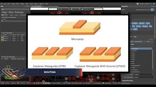
rf design in the pcb: transmission lines (coplanar)
Published 1 year ago • 11K plays • Length 2:40Download video MP4
Download video MP3
Similar videos
-
 4:59
4:59
rf design in the pcb: routing any angle or arc in altium designer
-
 10:55
10:55
board thickness in pcb design
-
 0:38
0:38
3 #pcbdesign strategies beginners should know #altium #electronics
-
 1:01:43
rf and microwave pcb design - part 5: couplers
-
 17:00
17:00
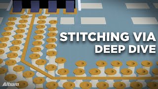
stitching via deep dive | pcb layout
-
 15:34
15:34
i2c and spi on a pcb explained!
-
 17:36
17:36
starting an rf pcb design
-
 21:05
21:05
(1) - rf and microwave pcb design - altium academy
-
 17:15
17:15
rf power amplifier design followup: pcb design
-
 41:18
41:18
(2) rf and microwave pcb design - transmission lines and impedance - altium academy
-
 2:51
2:51
rf design in the pcb: rf materials
-
 16:59
16:59
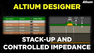
pcb stack-up and controlled impedance in altium designer
-
 1:00
1:00
super pro esp32 rf pcb layout: one minute #pcbdesign review 05 #electronics #altium
-
 21:40
21:40
how to design rf trace tapers (with free calculator!)
-
 12:52
12:52
top 5 beginner pcb design mistakes (and how to fix them)
-
 16:19
16:19
length tuning | pcb design basics tutorial
-
 18:52
18:52
types of copper in pcb design
-
 1:00
1:00
8-layer board? rockchip rk3328 pcb layout: one minute #pcbdesign review 08 #electronics #altium
-
 17:58
17:58
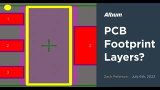
what's with all the layers in your pcb footprint?
-
 21:12
21:12
to pour or not to pour | copper pour in pcb design