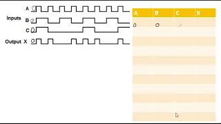
timing diagram of basic logic gates/ 2 input, 3 input and 4 input logic gate (nand)
Published 1 year ago • 1.5K plays • Length 10:38Download video MP4
Download video MP3
Similar videos
-
 3:18
3:18
basic logic gate timing diagram/ waveform of basic logic gate/digital electronics
-
 5:44
5:44
basic logic gate timing diagram: three input nand gate
-
 2:20
2:20
waveforms of basic logic gates | digital logic design | digital electronics | undergrad academy
-
 4:22
4:22
logic gate timing diagram /output waveform of basic logic gates/digital electronics
-
 36:41
36:41
eevblog #1249 - tutorial: timing diagrams explained
-
 5:42
5:42
logic circuit analysis using truth tables
-
 10:18
10:18
digital logic circuit design by given input and output waveform/ digital logic
-
 4:24
4:24
output timing diagram of basic logic gate (four input nand gate)
-
 5:01
5:01
basic timing diagrams for combinational logic circuits
-
 5:30
5:30
basic or logic gate output timing diagram/ digital logic
-
 3:39
3:39
basic timing diagrams
-
 3:21
3:21
output timing diagram of three input xor gate when all inputs are in waveform form
-
 54:07
54:07
logic gates, truth tables, boolean algebra and, or, not, nand & nor
-
 10:49
10:49
output waveform of basic logic gate / digital logic design
-
 0:33
0:33
creative ideas for logic gates
-
 4:47
4:47
output of three input nor gate when all inputs are in waveform form
-
 3:48
3:48
output waveform of nand gate/ basic logic gate output waveform/digital electronics