tip #092: under a component with exposed pad (ep), you may want to ...
Published 7 years ago • 8.3K plays • Length 4:43Download video MP4
Download video MP3
Similar videos
-
 3:51
3:51
tip #014: if you have an exposed pad on your component, consider ...
-
 3:02
3:02
tip #095: you may want to place all the components on the board before you start doing layout
-
 1:18:48
using via in pad? what you need to know - guidelines, dimensions and more ...
-
 1:15:31
how to select and place esd components to protect your boards?
-
 5:17
5:17
tip #091: in schematic, mark the components which you may not want to fit
-
 52:27
52:27
headstart's pc with the weird gui "os" [explorer]
-
 8:33
8:33
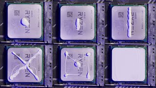
best way to apply thermal paste? does it even matter?
-
 3:50
3:50
types of pcb pads | pcb knowledge
-
 5:10
5:10
tip #089: when desoldering, don’t be afraid of using a lot of solder
-
 5:32
5:32
tip #099: your product should be tested for esd discharge
-
 43:53
43:53
3 simple tips to improve signals on your pcb - a big difference
-
 3:56
3:56
tip #085: if you don’t have space on pcb, consider to use stands off components
-
 0:16
0:16
this chapter closes now, for the next one to begin. 🥂✨.#iitbombay #convocation
-
 2:58
2:58
tip #090: crystals can be placed also on the opposite side of pcb, just keep the tracks short
-
 2:46
2:46
tip #027: use at least 2 monitors
-
 4:35
4:35
tip #063: consider to place analogue circuits in corners of your pcb
-
 4:30
4:30
tip #009: choose two or three biggest component suppliers ...