two-layer pcb design tips: achieving the optimal layout
Published 4 months ago • 9.3K plays • Length 21:32Download video MP4
Download video MP3
Similar videos
-
 10:57
10:57
the most common 2-layer pcb design mistakes and how to avoid them
-
 12:52
12:52
top 5 beginner pcb design mistakes (and how to fix them)
-
 14:01
14:01
voltage regulator layout on a 2-layer board | pcb routing tips
-
 32:27
32:27
2-layer pcb design tips - phil's lab #137
-
 14:41
14:41
high-speed routing on a two-layer board
-
 10:40
10:40
6 horribly common pcb design mistakes
-
 13:52
13:52
should you put an inductor above ground? | pcb layout
-
 32:45
32:45
how to create a new multi-board project in altium designer
-
 0:53
0:53
could do this in 2 layers! | 1-min #pcbdesign review
-
 6:32
6:32
wearable design project - part vi: pcb layout part ii
-
 15:07
15:07
qfn layout and routing - tips & tricks
-
 18:12
18:12
types of pcb grounding explained | pcb layout
-
 21:12
21:12
to pour or not to pour | copper pour in pcb design
-
 17:58
17:58
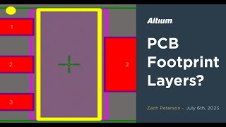
what's with all the layers in your pcb footprint?
-
 0:27
0:27
4 strategies to keep your pcb layer count low #pcbdesign #electronics #altium
-
 0:59
0:59
best and worst pcb design software
-
 14:54
14:54
pcb layout planning - how to decide on what layers we should use
-
 17:00
17:00
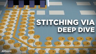
stitching via deep dive | pcb layout
-
 0:38
0:38
3 #pcbdesign strategies beginners should know #altium #electronics
-
 0:33
0:33
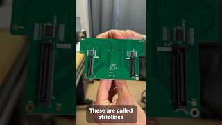
striplines vs. microstrips - what’s the difference in #pcbdesign? #electronics #altium
-
 18:54
18:54
how gnd vias improve your pcb layout