van der waals heterostructure devices for tunneling phototransistor and electronic spectroscopy
Published 3 years ago • 440 plays • Length 1:16:20Download video MP4
Download video MP3
Similar videos
-
 7:53
7:53
van der waals heterostructures
-
 37:52
37:52
cefipra project: optoelectronics in van der waals heterostructures – fundamentals to quantum devices
-
 40:00
40:00
remote electron-phonon interactions and screening in van der waals heterostructures (t. sohier)
-
 40:04
40:04
tunable electronic and optical properties in rotatable heterostructures | 2022 nss americas
-
 1:02:03
luis a. jauregui: novel optoelectronic devices based on van der waals heterostructures
-
 47:20
47:20
the field-free josephson diode effect in a van der waals heterostructure, by heng wu
-
 38:14
38:14
electronic excitations in two-dimensional materials and van der waals heterostructures
-
 40:27
40:27
spectroscopy and transportin 2d materials
-
 41:01
41:01
fdns21: realizing 2d transport in 2d van der waals crystals
-
 1:04
1:04
spectroscopy in :60 - deltadiodes™
-
 1:07:11
geometry and the design of van der waals 2d heterostructure
-
 1:45
1:45
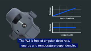
exradin w2 scintillator overview
-
 56:11
56:11
spectroscopy of topological materials: photoemission and tunneling spectroscopy
-
 3:01
3:01
⚡️⚡️⚡️what is photonic intergrated circuit⚡️⚡️⚡️
-
 35:17
35:17
van der waals heterostructures of 2d materials | emanuel tutuc
-
 8:16
8:16
nanodiffraction and surface diffraction
-
 38:11
38:11
correlated states in van der waals heterostructures by abhay narayan pasupathy
-
 17:31
17:31
“thickness-dependent tunneling spectra of 2h-tas₂” by shahar simon