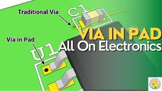
via-in-pad design | pcb knowledge
Published 1 year ago • 13K plays • Length 3:09Download video MP4
Download video MP3
Similar videos
-
 4:07
4:07
what are thermal relief pads? | pcb knowledge
-
 3:19
3:19
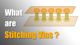
what are stitching vias? | pcb knowledge
-
 3:52
3:52
what is a pcb via? | pcb knowledge
-
 3:50
3:50
types of pcb pads | pcb knowledge
-
 16:10
16:10
when to use via in pad
-
 2:11
2:11
via-in-pad for bga
-
 1:18:48
using via in pad? what you need to know - guidelines, dimensions and more ...
-
 10:31
10:31
using vias in pads in your designs
-
 13:12
13:12
how pcb is made in china - pcbway - factory tour
-
 10:40
10:40
6 horribly common pcb design mistakes
-
 30:11
30:11
how to improve your pcb layout - vias
-
 4:13
4:13
do you need non-functional pads? | pcb knowledge
-
 17:01
17:01
pcb vias 101 - phil's lab #77
-
 2:15
2:15
what is stiffener in flexible pcbs ? | pcb knowledge
-
 3:22
3:22
what is pcb back drilling? | pcb knowledge
-
 0:33
0:33
pad and via styles in altium designer
-
 4:05
4:05
what are pcb teardrops? | pcb knowledge
-
 6:34
6:34
how to create and asign new vias in pads layout
-
 2:04
2:04
what are the castellated holes in pcb? | pcb knowledge
-
 11:13
11:13
via2pad pcb - connect circuit boards together with a via and a pad!
-
 2:54
2:54
what are mounting holes? | pcb knowledge
-
 0:25
0:25
via plugging (via in pad – conductive or non-conductive) (best tutorials in 2021)