ymtc introduces x3 9070 3d nand flash powered by innovative xtacking 3 0 architecture
Published 2 years ago • 196 plays • Length 1:24Download video MP4
Download video MP3
Similar videos
-
 1:32
1:32
3d nand: key process steps
-
 5:22
5:22
historical development! china's ymtc produces the world's most advanced 3d nand memory chip
-
 1:28
1:28
chinese ymtc achieves mass production of 232 layer 3d nand, beating kioxia, micron, samsung, and sk
-
 2:07
2:07
ymtc's mysterious flash memory exposed! break through the us ban!
-
 1:12
1:12
toshiba 3d nand chip | product video | explainer video
-
 7:41
7:41
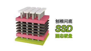
深入理解闪存!固态硬盘如何存储一位数据?nand flash是怎么擦除和写入的?flash的工作原理!
-
 9:55
9:55
basic skills for mobile repair section 4 how to remove cpu and emmc safely
-
 17:12
17:12
how to copy software using rt809h jtag to tp.ms358.pb802 smart board #how #howtorepair #smart #logo
-
 2:21
2:21
3d nand vs 2d nand: what's the difference in nand flash memory?
-
 3:23
3:23
kioxia bics flash™ generation 8 3d flash memory makes the most of cba technology
-
 4:04
4:04
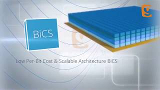
kioxia memory technology - bics flash™ 3d flash memory concept
-
 5:16
5:16
3d nand as fast as possible
-
 6:58
6:58
the power of the chip - how china’s ymtc leap-frogged the competition
-
 5:19
5:19
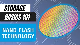
nand flash technology | swissbit storage basics 101 | nand flash memory basics explained
-
 3:51
3:51
building for the future with the power of 3d nand
-
 2:46
2:46
3d nand: the future of flash
-
 2:51
2:51
understanding 3d flash memory: layers vs cost/performance (part 2)
-
 2:40
2:40
kioxia slc nand flash memory
-
 5:20
5:20
what’s the difference between slc, mlc, tlc and 3d nand? - diy in 5 ep 159
-
 7:34
7:34
yangtze memory technology (ymtc) cctv ”dialogue” with mr zhao
-
 1:05
1:05
ymtc to supply nand flash chips to lexar
-
 5:30
5:30
micron first to market with 232 layer nand - episode 133 - six five