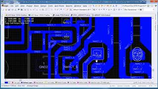
electronics: altium: polygon pour direct connect on vias, relief connect on pads (2 solutions!!)
Published 2 years ago • 35 plays • Length 3:20Download video MP4
Download video MP3
Similar videos
-
 1:30
1:30
altium polygon pour direct connect
-
 0:42
0:42
how to connect polygons to nets in altium designer
-
 0:59
0:59
what is a thermal relief pad on a pcb?
-
 1:18:47
using via in pad? what you need to know - guidelines, dimensions and more ...
-
 10:41
10:41
altium designer-build polygon
-
 21:12
21:12
to pour or not to pour | copper pour in pcb design
-
 2:25
2:25
how to change polygon connect styles in altium designer | pcb layout
-
![altium designer [design rules polygon connect style]_1](https://i.ytimg.com/vi/kLxDrbyPo8s/mqdefault.jpg) 9:51
9:51
altium designer [design rules polygon connect style]_1
-
 3:45
3:45
how to create polygons in altium designer | pcb layout
-
 5:58
5:58
thermal connection styles - altium academy
-
 1:54
1:54
how to route with vias in altium
-
 3:32
3:32
11.2 polygon pours gnd altium designer
-
 16:10
16:10
when to use via in pad
-
 8:33
8:33
how to design rotation-proof connector pinouts
-
 0:46
0:46
dynamic copper polygon management tools in altium designer 17
-
 3:46
3:46
how to use the polygon manager in altium designer
-
 0:49
0:49
auto cross-probing in altium designer 17 - pcb design software
-
 2:35
2:35
polygon pour in altium designer | pcb routing