polygon pour in altium designer | pcb routing
Published 2 years ago • 15K plays • Length 2:35Download video MP4
Download video MP3
Similar videos
-
 3:45
3:45
how to create polygons in altium designer | pcb layout
-
 2:51
2:51
snapping when creating polygons in altium designer | pcb routing
-
 3:45
3:45
how to edit polygons in altium designer | pcb routing
-
 0:42
0:42
how to connect polygons to nets in altium designer
-
 21:12
21:12
to pour or not to pour | copper pour in pcb design
-
 3:38
3:38
how to change polygon types in altium designer | pcb layout
-
 8:04
8:04
adding polygon pour in pcb design using altium designer, modify, remove a section of polygon pour
-
 1:34:41
altium designer 22 tutorial - quick & easy | step by step
-
 21:20
21:20
microcontroller-based hardware design with altium designer - #1 introduction and part selection
-
 47:31
47:31
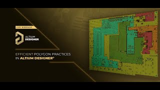
webinar: efficient polygon practices in altium designer®
-
 12:28
12:28
how to make polygon pours and cutouts more professional
-
 1:05
1:05
using polygons on power planes | altium designer 21 what's new
-
 8:27
8:27
(7) routing the pcb - altium designer
-
 18:47
18:47
microcontroller-based hardware design with altium designer - #9 pcb routing tips
-
 13:27
13:27
floods, planes and polygons for ground and power | altium designer 17 essentials | module 24
-
 2:25
2:25
how to change polygon connect styles in altium designer | pcb layout
-
 3:46
3:46
how to use the polygon manager in altium designer
-
 2:02
2:02
introduction to snapping options in altium designer | pcb routing
-
 23:37
23:37
altium designer quick-start tutorial with phil salmony from phil's lab