snapping when creating polygons in altium designer | pcb routing
Published 2 years ago • 2.3K plays • Length 2:51Download video MP4
Download video MP3
Similar videos
-
 3:45
3:45
how to create polygons in altium designer | pcb layout
-
 3:45
3:45
how to edit polygons in altium designer | pcb routing
-
 2:35
2:35
polygon pour in altium designer | pcb routing
-
 2:02
2:02
introduction to snapping options in altium designer | pcb routing
-
 2:03
2:03
snapping when creating routes in altium designer | pcb routing
-
 10:40
10:40
6 horribly common pcb design mistakes
-
 43:14
43:14
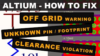
altium - how to fix: off grid warning, missing footprint, unknown pin, clearance violations
-
 17:00
17:00
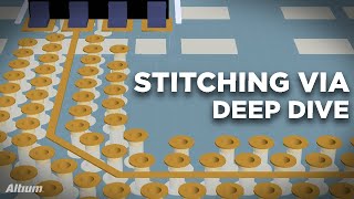
stitching via deep dive | pcb layout
-
 1:50
1:50
how to set snap distance & snap range in altium designer | pcb layout
-
 1:58
1:58
creating guide lines and snap points in altium designer | pcb layout
-
 0:42
0:42
how to connect polygons to nets in altium designer
-
 2:48
2:48
how to use snapping for primitives and components in altium designer
-
 25:58
25:58
best practices: efficient use of snapping in altium designer
-
 8:27
8:27
(7) routing the pcb - altium designer
-
 1:05
1:05
using polygons on power planes | altium designer 21 what's new