what to consider when designing edge connectors
Published 1 year ago • 18K plays • Length 4:09Download video MP4
Download video MP3
Similar videos
-
 17:41
17:41
pcb edge plating guidelines
-
 21:35
21:35
(2) introduction to multiboard pcb design - connectors - altium academy
-
 0:38
0:38
3 #pcbdesign strategies beginners should know #altium #electronics
-
 12:52
12:52
top 5 beginner pcb design mistakes (and how to fix them)
-
 13:18
13:18
should you remove ground below an sma connector?
-
 10:40
10:40
6 horribly common pcb design mistakes
-
 17:00
17:00
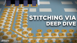
stitching via deep dive | pcb layout
-
 21:32
21:32
two-layer pcb design tips: achieving the optimal layout
-
 11:30
11:30
how to arrange connectors and pinouts
-
 3:59
3:59
how to improve your pcb designs with queries & rules
-
 1:00
1:00
rearrange some components! one minute #pcbdesign review 15 #electronics #altium
-
 3:11
3:11
how to set copper to edge clearance in altium designer
-
 17:53
17:53
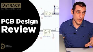
pcb design review deep dive
-
 8:33
8:33
how to design rotation-proof connector pinouts
-
 17:58
17:58
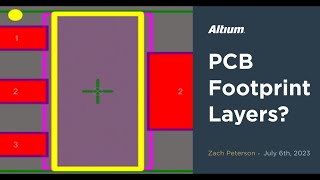
what's with all the layers in your pcb footprint?
-
 12:45
12:45
3 types of pcb manufacturing output files you need to know
-
 0:54
0:54
nice use of thermals! 1 min pcb design review
-
 15:58
15:58
(1) introduction to multiboard pcb design - altium academy
-
 0:27
0:27
4 strategies to keep your pcb layer count low #pcbdesign #electronics #altium
-
 17:36
17:36
starting an rf pcb design
-
 8:34
8:34
the pcb shape and outline | altium designer 17 essentials | module 17