where to place snubbers in a buck converter
Published 2 years ago • 6.2K plays • Length 13:55Download video MP4
Download video MP3
Similar videos
-
 12:33
12:33
what is a fly-buck converter?
-
 5:54
5:54
buck converter
-
 16:15
16:15
how to run a simulation of buck converter - pcb design
-
 15:08
15:08
how to design an rcd snubber (a.k.a. rcd clamp)
-
 19:41
19:41
electronic switches - smps and snubbers (2/2)
-
 18:34
18:34
electronic switches - smps and snubbers (1/2)
-
 3:41
3:41
how to place pcb prototype order---pcbway review by ddelectrotech
-
 23:33
23:33
microcontroller-based hardware design with altium designer - #2 buck converter
-
![buck converter circuit simulation [altium designer]](https://i.ytimg.com/vi/VTgiHjXXGL8/mqdefault.jpg) 14:43
14:43
buck converter circuit simulation [altium designer]
-
 10:44
10:44
what is a snubber circuit and how to design it? | power electronics
-
 0:33
0:33
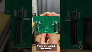
striplines vs. microstrips - what’s the difference in #pcbdesign? #electronics #altium
-
 3:40
3:40
how to place connections between boards in altium designer
-
 0:55
0:55
enable port isn't going anywhere! 1 min buck converter design review
-
 7:20
7:20
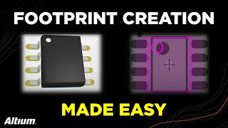
pcb footprint creation made easy (ipc compliant footprint wizard)
-
 10:11
10:11
should you route gnd or pe through a connector?
-
 0:43
0:43
how to insert transmission line table for impedance controlled fabs in draftsman | altium designer
-
 12:57
12:57
how to place cavity regions in your pcb footprint
-
 0:51
0:51
tenting vias in altium designer
-
 0:59
0:59
measuring ground difference in isolated flyback converters