why chiplet will transform the semiconductor ecosystem from design to packaging?
Published 1 month ago • 213 plays • Length 14:46Download video MP4
Download video MP3
Similar videos
-
 5:16
5:16
‘semiconductor ecosystem’ explained | 'all about semiconductor' by samsung semiconductor
-
 17:18
17:18
known good die is at the heart of a sustainable open chiplet business model
-
 7:44
7:44
‘semiconductor manufacturing process’ explained | 'all about semiconductor' by samsung semiconductor
-
 8:00
8:00
chiplet innovation ecosystem
-
 30:10
30:10
panel: what is next in building the open chiplet economy
-
 14:59
14:59
advanced packaging platforms and design kits for chiplets integration in hpc applications
-
 23:01
23:01
inside micron taiwan’s semiconductor factory | taiwan’s mega factories ep1
-
 8:40
8:40
how are billions of microchips made from sand? | how are silicon wafers made?
-
 14:32
14:32
chiplets: divide and conquer | the future of processors
-
 19:08
19:08
chiplets for addressing challenges and use cases for ai and ml applications
-
 14:15
14:15
ai/hpc: advanced package tech. for chiplet adoption and memory integration in hpc/ai applications
-
 18:52
18:52
using cdxml/jep30 models for chiplet design and verification
-
 20:42
20:42
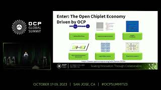
building an open chiplet economy
-
 2:28:58
joint ocp & jedec workshop - standards for chiplet design with 3dic packaging - day 1 (2024-06-14)
-
 29:26
29:26
ocpreg19 - the impact of domain specific acceleration and chiplet technology on the semiconductor an
-
 59:10
59:10
tsp #247 - world's largest microwave industry exhibition - ieee microwave symposium, washington 2024
-
 35:30
35:30
ocpreg19 - accelerating innovation through chiplets and the advanced interface bus (aib)
-
 9:23
9:23
building the open chiplet economy
-
 29:30
29:30
road to chiplets: architecture - jan vardaman: why chiplets?
-
 12:53
12:53
why amd's chiplets work
-
 23:47
23:47
the rise of chiplets in advanced ai / ml / hpc soc's - presented by credo semiconductor